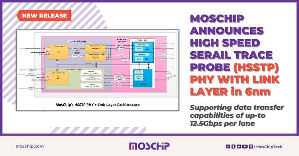
Supporting data transfer capabilities of up-to 12.5Gbps per lane
Santa Clara, CA: MosChip Technologies, a semiconductor and system design services company, unveils today enhanced simplex High Speed Serial Trace Probe (HSSTP) PHY macro with link layer supporting data transfer capabilities of up-to 12.5Gbps per lane in 6nm FinFET technology. MosChip has over a twenty-year track record in designing semiconductor IP, products, and SoCs for Computing, IoT, networking, industrial, and consumer applications.
MosChip was the first fabless semiconductor company out of India and has developed many connectivity-based products that were fabricated at leading foundries and shipped in millions of units. With the acquisition of Gigacom in 2018, the company has developed a niche expertise in the areas of analog, mixed-signal design, high- speed serial interfaces, and IP portfolio which includes silicon proven SerDes, PLLs, and Data converters. The multi-lane HSSTP is part of MosChips’ transceiver portfolio, meeting the growing needs for higher bandwidth trace with fewer SoC pins.
“MosChip’s HSSTP IP can be paired with any HSSTP compatible receiver system to create a flexible debugging platform customizable for nearly every silicon bring-up strategy” said Swamy Irrinki, VP of Marketing and Business Development at MosChip. HSSTP PHY and Link Layer enables High-Speed Debug/Test data transfer, Real-Time monitoring of on-chip signals/bus and Silicon Debug for advanced FinFET SoCs with high performance Arm® CPU cores.
To enable the capture of multiple lanes of high-speed serial trace, Arm® has created the HSSTP trace probe which is ideal for situations where it’s necessary to collect a large amount of trace data and/or where SoC termination count rules out parallel trace. MosChip’s HSSTP link layer is one of the components of the standard Serial Trace Port (STP) within the Arm®CoreSight ecosystem. The Trace Port Interface Unit (TPIU) sends data through an STP that can use a serial high-speed interface (SERDES). TPIU interface complies with the Arm® CoreSight protocol and Link layer complies with the Aurora 8b/10b Simplex specification.
“This is a major milestone for MosChip, which highlights our strategic focus to develop niche SerDes PHY IP as per customer requirements,” said Venkata Simhadri, MD/ CEO of MosChip. Successful silicon tape-out of HSSTP PHY with link layer in 6nm also demonstrates MosChip’s design flow and methodology in advanced FinFET nodes.
HSSTP PHY macro deliverables include a complete set of logical views, physical views, documentation, Verilog model, verification environment, an abstract view, liberty files, netlist, GDSII and flip chip bump/ball map plans. HSSTP Link layer deliverables include RTL Verilog, Synthesis/ Timing SDC, and Test Bench


